What is Continuous Drain Current on a Mosfet
The post comprehensively explains the current rating of MOSFETs in their datasheets, and helps us to understand how it is calculated by the design engineers, keeping in mind the various external parameters, which potentially impact the current limitations of the device.
In simple terms, MOSFET current rating can be defined as the maximum amount of current a MOSFET can handle safely and optimally across its drain to source terminals, with its case temperature held below 40 °C.
The Current rating is perhaps the most deceiving parameter on a MOSFET datasheet, since you cannot find any industry standard technique to precisely evaluate this parameter.
Although there may be different approaches for estimating this, the descriptions can be apparently varied and misleading across different brands and manufacturers. Which is the reason it's important to look at the footnotes wherever these are available, to know exactly where these ratings originated from.
Another truly essential factor to remember is that, in any datasheet the transistor current ratings are just entirely calculated figures. These are definitely not measured by an equipment, nor are these verified part by part during the production process.
To implement the current rating calculations, it is important to consider specific issues related to the circumstances which the device will likely be subjected to, for example the PCB assembly factor of the designer, the thermal surroundings etc. Therefore each of these parameters may not be commonly relevant for every single MOSFET?
The final thing to note is that current ratings effects many of the additional statistics down the road within the datasheet. Therefore even when they may be calculated, all those computations could include ramifications for some other variables and stats.
Absolute Maximum Current Ratings
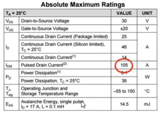
The MOSFET current ratings could be found basically, in the Absolute Maximum Ratings Table as indicated in the figure below:.
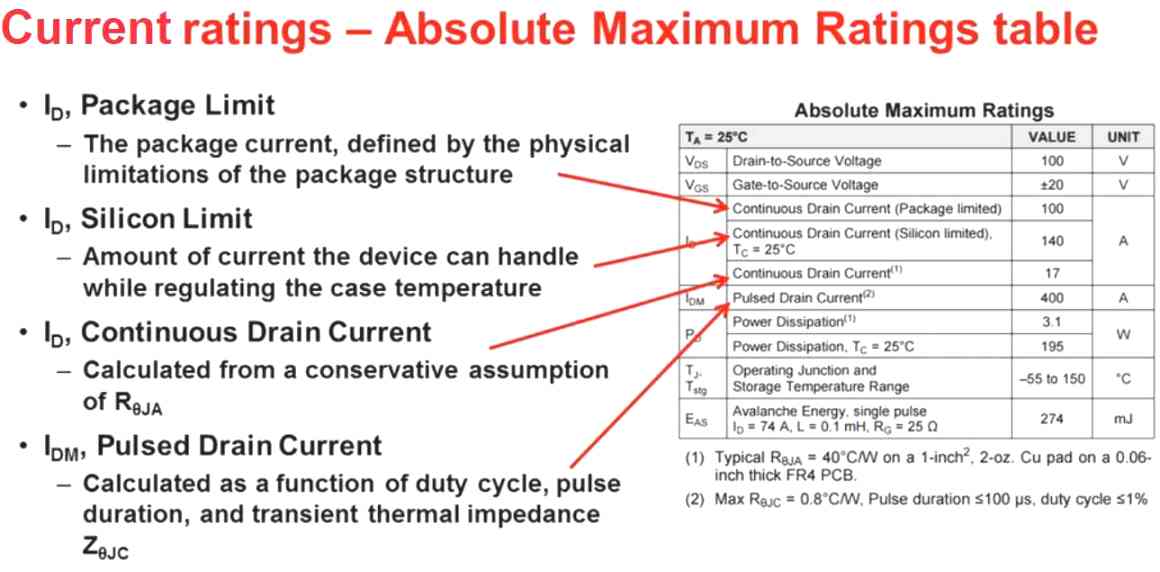
Thus when we focus into our Absolute Maximum Table, we are able to see these are actually classified by 4 separate current limiting factors for the same device.
- Package Limit
- Silicon Limit
- Continuous Drain Current
- Pulsed Drain Current
Let's learn each of those parameters in greater depth.
At the beginning, we see the package current limit, which signifies the limit characterized by the practical external limitations of the MOSFET package itself.
Next comes the silicon current limit, which is characterized by the magnitude of current which the silicon die of the device can practically tackle, as soon as the MOSFET case temperature attains a specific value.
Here, this is presented considering the device case temperature held at 25 °C. Other suppliers may possibly offer this at some different temperature level. For Texas Instrument T-0220 MOSFETs, for example, this is presented at 25 °C, and also 100 °C case temperature.
Below this temperature level, there may be an additional continuous current rating, calculated with safe tolerance margins, with regards to the specific device's junction to ambient thermal impedance.
After that lastly, instead of a continuous current, we find a pulsed current rating included, which is, actually, calculated relative to both duty cycle and pulse duration. And hence for sure, the thermal impedance of the device.
Now let's understand all the above MOSFET current limitations with an in-depth detail. We will start with the package current limit of the device.
Package Current Limit
The package current limit, as we discussed earlier, depend on the true restrictions of the device package itself, and the internal chip connections between the silicon die and the plastic package or lead frame.
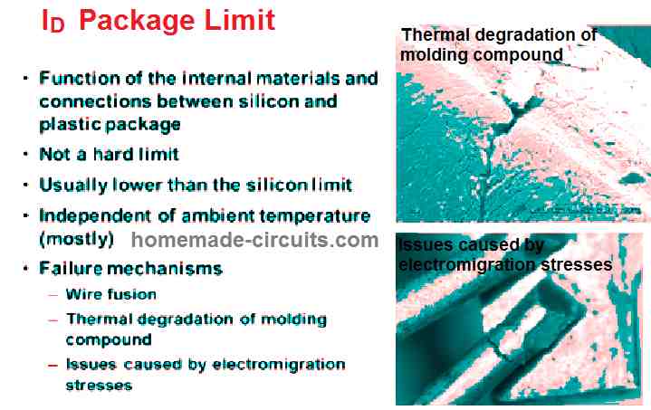
Having said that, this current limit parameter is not actually a final limit. Meaning, if the MOSFET package is rated to handle 50 amp current, it doesn't mean that exceeding 50 amps, will suddenly cause an explosion of the device. The 50 amp value may actually signify that, if the FET current is exceeded above this value, the effects could be unpredictable, and this may possibly reduce the long-term reliability of the device.
Therefore you can apply higher current than the specified package limit, if, perhaps you are able to maintain the MOSFET case temperature sufficiently cool, so that it remains under the maximum allowable thermal limitation value. That said, frequently crossing the package limit could endanger the long-term reliability of the device to a great extent.
Typically, the package limit is usually below the calculated silicon limit. This may not be always true for the higher-resistance devices. Nevertheless generally, the package limit could be considered as the limit that is outlined with greater cautiousness and greater +/- margin than the silicon limit.
The package current limit is generally not dependent on the ambient temperature conditions? It is more dependent on the temperature that's just close by between the internal connections, which leads to the thermal compression and expansion, and eventually deterioration of those connections.
Therefore, the situation may lead to the breaking of the internal connecting wires due to extensive thermal expansion and shrinkage.
Additional breakdown factors consist of wire melting when they get exceedingly hot by themselves, due to huge current flow; thermal wreckage of the molding element that holds the wires attached to the lead frame; and various other complications attributable to electromigration strains of the real electrons flow.
Silicon Current Limit
However if we consider the silicon current limit of a MOSFET it may appear a lot more relevant and genuine current limitation. Because it assumes that you could keep the MOSFET case temperature to a particular level, since this calculation is carried out from the junction-to-case thermal impedance, in contrast to the junction-to-ambient thermal impedance.
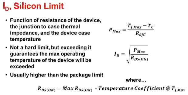
Therefore basically, what is assumed in the silicon current limit is an overly ideal heatsinking condition, which is able to hold the case-to-ambient thermal impedance effectively to 0. This may be equivalent to immersing the MOSFET inside liquid nitrogen, which could be practically impossible. Right?
However the above scenario provides some clue regarding thermal performance, at least over a relative degree from MOSFET to MOSFET.
Yet again, it's not actually a strict limit, although it can be definitely never encouraged exceeding this current limit, which would otherwise mean crossing the maximum allowable temperature limit. This could in turn result in your MOSFET bursting, or it might simply cause a massive degradation of the device, along with adversely affecting the long-term reliability of the MOSFET.
Calculating Power Dissipation
Let's examine how the calculations are worked out. We will begin by figuring out the maximum permissible power dissipation PMax of the device.
As discussed before this will be from the junction-to-case thermal impedance, and using the delta (Tj,Max - TC ) of the maximum allowed junction temperature to the case temperature which we assume to keep the case temperature at.
PMax = Tj,Max - TC / RθJC (Equation#1)
- where Tj,Max is the maximum junction temperature of the MOSFET,
- RθJC = junction-to-ambient thermal impedance of the MOSFET
- and TC is the case temperature of the MOSFET
ID = √ PMax / RDS(ON) (Equation#2)
where,
RDS(ON) = Max RDS(ON) x Temperature Coefficient @ Tj,Max (Equation#3)
Once again, this will be generally 25 °C, although not exactly always. Following this, the calculation is simply a fundamental P = I2R equation which allows us to find out the drain current of the device.
The Role of RDS(ON)
We can see the parameter RDS(ON) incorporated in this equation here, which is the maximum drain to source resistance value of the MOSFET on the datasheet. Typically, it can be the optimum resistance at the maximum possible gate voltage. For example, when we use RDS(ON) at 4.5 milliohms, and 10 volts for a selected part, we take the 10 volt maximum resistance into consideration .
However, it will be also important to multiply this figure with the temperature coefficient at the maximum junction temperature. Mainly because, we have assumed that the silicon die would become hot, up to its maximum allowable temperature, at this rating.
Temperature Coefficient at the Maximum Junction Temperature
You may find this curve in all Texas Instrument MOSFET datasheets.
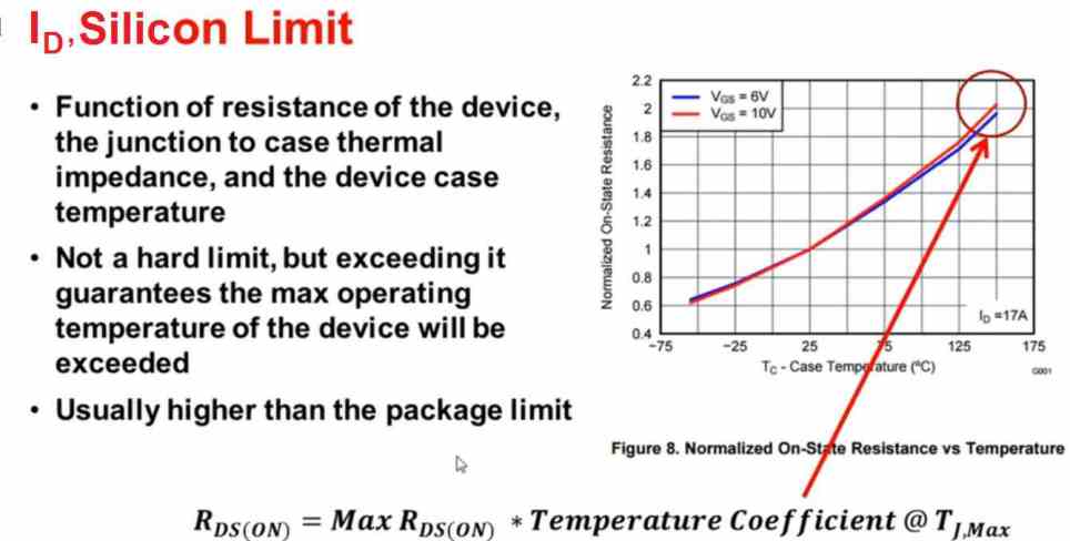
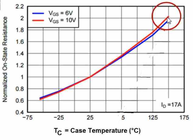
This curve is the device's drain/source normalized resistance value versus its case temperature value. In the above graph, we find that if the maximum case temperature of the MOSFET reaches upto 150 °C, it might cause the drain/source resistance of the device to climb to 2 Ohms which seems to be twice the resistance value at the 25 °C mark. Therefore, we have to consider this maximum resistance value 2 and multiply it with our Max RDS(ON) , to get the MOSFET resistance at its maximum allowable junction temperature.
And this is the resistance that's employed in this Equation#3. This resistance value is not only implemented in the silicon limit current formula, but also in all of the current limit calculations. Meaning, we always consider the maximum resistance RDS(ON) of the device at its maximum case temperature.
After this, we have one more continuous drain current limitation, on this occasion, determined by the junction-to-ambient thermal impedance of the MOSFET. Meaning, this current limitation is going to be described at a particular ambient temperature, in the present situation, this will be usually the room temperature, or at 25 °C. This will be normally indicated at the footnote, regarding what exactly RθJA, junction-to-ambient, thermal impedance was assumed for this specific calculation.
What is RθJA?
Now, what is RθJA? It is a value which is far more dependent on the circuit board layout of the designer, compared to the MOSFET parameter itself.
Therefore for this limitation the manufacturer has to assume the possible board layout parameters on which the MOSFET would be installed by a potential user.
Now, with the board layout assumptions the manufacturer has to be very cautious again. For example, to be on the safer side it may be assumed to consider a junction-to-ambient thermal impedance of 40 °C per watt. But on the other hand, possibly the user may have a PCB layout designed with much superior RθJA than the assumed 40 °C per watt. That would then allow the user to use higher current levels through their MOSFET than the indicated limit on the datasheet?
Still, even in such scenarios, the specified conservative (subdued) value of RθJA in the datasheet would be the safest recommended current limit for the MOSFET.
Now, RθJA could be as much as 2 times higher than our assumed RθJC therefore this magnitude could naturally be a lot lower compared to calculated silicon limit of the MOSFET.
You may not find this RθJA for all the MOSFET packages that are released by the Texas Instrument. For example, since the TO-220 devices are normally fitted on large heat sinks in real life applications, the RθJA practically will be nearer to the RθJC value compared to the value which may be offered on the datasheet. And therefore, this type of current limit may not necessarily indicative of the amount of current the device could handle in a real life usage. It possibly might manage to handle higher than the 62 °C per watt RθJA value presented on the data sheet.
Pulsed Drain Current Limit
Finally, now we arrive at the pulsed drain current limitation parameter, or IDM, which refers to the maximum amount of current the MOSFET is able to tolerate, using shorter gate pulse periods or with a specific duty cycle instead of constant DC operation.
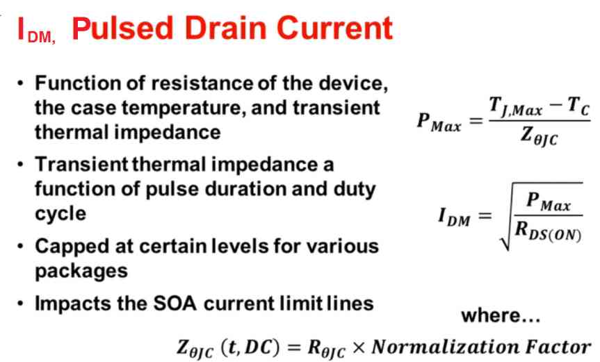
Referring to the equations, we find them all identical to out earlier Equation#1, except for the normal RθJC which is now replaced with ZθJC.
PMax = Tj,Max - TC / ZθJC (Equation#4)
ZθJC is known as the transient thermal impedance, which is actually the normal thermal impedance multiplied by certain normalization element, with regard to the pulse duration, and also the duty cycle.
ZθJC (t, DC) = RθJC x Normalization Factor (Equation#5)
Depending on the package type. this current limit are specified differently. For example, for the TO-220s 5 x 6 QFNs are designated at 400 amps maximum, since forcing the package limit any further than 400 amps appeared unrealistic and too stressful, for any MOSFET to handle.
This is why, in particular, the pulse current limitations of a FET device would be the limitations which normally outline the SOA current limit lines.
Recalling from one of our earlier posts, every single pulse duration indicated in the SOA signified a distinctive current limitation magnitude. That's where the pulse current limitation lines are usually calculated. Nevertheless these are usually assigned at 400 amps, for TO-220 devices and 5 x 6 QFNs.
Practical Example
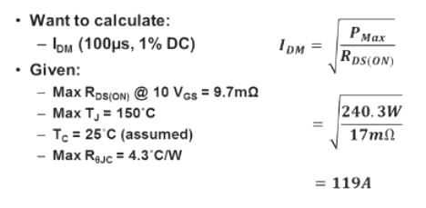
Now let's evaluate a real MOSFET CSD17579Q5A example for figuring out the pulse current. This is a 30-volt, 5 x 6 QFN MOSFET. And let's imagine we would like to determine the current with specifications as featured on the front page of the datasheet, that happen to be 100 microseconds and 1% duty cycle.
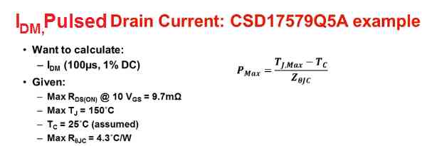
We can quickly grab the given available from the datasheet, as indicated above. We have the maximum resistance of the CSD17579Q5A , at 10 volts Vgs, to be 9.7 milliohms, as foreseen in the datasheet electrical characteristics table.
In the the Absolute-Maximum table we discover that the maximum allowable junction temperature for this device is 150 °C. Likewise if we refer to the thermal data table we realize that the maximum RθJC for this device is 4.3 °C per watt.
Calculations
Now, we have reached the point where we can begin our calculations. First of all we have to find out what this transient thermal impedance value is.
Looking at the figure 1 in the datasheet (zoomed in the below image) we are able to visualize what our normalization factor is, which needs to be multiplied with our continuous thermal impedance.
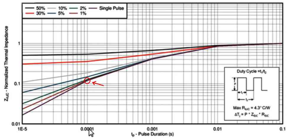
Thus considering these factors, we look at the 100 microseconds (0.0001 seconds) figure. And after that we focus on the line which indicates 1% duty cycle, represented as the brown line. And we discover a normalization factor of approximately 0.12, that we multiply by our 4.3 °C per watt to generate a transient thermal impedance of 0.52 °C per watt. And finally we divide that into our temperature delta to determine the amount of power as 240 watts, which can be dissipated by this MOSFET, for this pulse period and duty cycle.
PMax = Tj,Max - TC / ZθJC
= 150 °C - 25 °C / 0.12 x 4.3 °C/W
= 125 °C / 0.52 °C/W
= 240.3 watts
The final data we want to determine is, to what extent this maximum resistance of the device could rise at the maximum 150 °C case temperature.
Therefore we refer to the figure 8 of the datasheet. In this graph, we search for our temperature coefficient value, which seems to be around 1.75, corresponding to the 150 °C temperature point (as shown below).
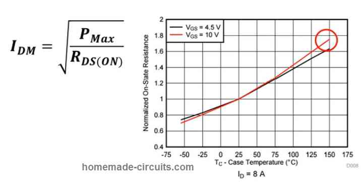
Therefore, we can now multiply our maximum resistance with this 1.75 temperature coefficient value, to get the RDS(ON) at 150 °C.
RDS(ON) = Max RDS(ON) x Temperature Coefficient @ Tj,Max
= 9.7 mΩ x 1.75 = 17 mΩ
We get the result as 17 milliohms, which explains that at the maximum 150 °C, breakdown limit, the RDS(ON) resistance of this MOSFET could possibly maximize up to 17 milliohms.
After this, using the above conditions we are now able to quickly calculate the maximum tolerable pulse current as 119 amps, as shown below.
ID = √ PMax / RDS(ON)
= √ 240.3 / 17 mΩ = 119 A
Comparing with Datasheet Results
However, now it will be important to check, whether or not this 119 amp value actually matches with the relevant figure presented on the front page of the datasheet? The answer seems to be negative,
NO! it doesn't. On the datasheet front page we find the equivalent value to be only 105 amps. Why so?
The reason behind this could be hidden in our SOA table of the datasheet.
Referring to the SOA table below we find that unlike the longer pulse duration lines which ranges between 10 milliseconds or 1 millisecond, the smaller 100 microsecond line seems to hit the MOSFET's max RDS(ON) line, even before it is able to touch our 119 amp limit.
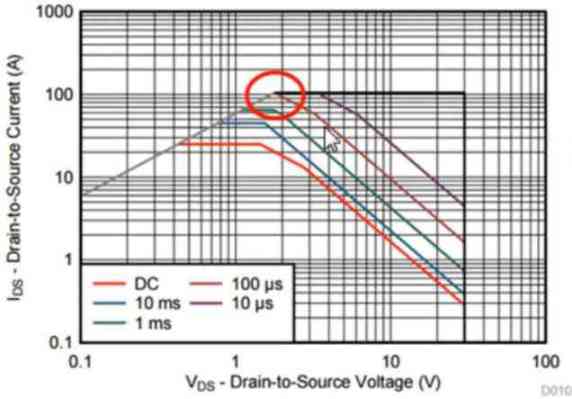
This simply means that, the real resistance of the MOSFET is actually limiting the amount of current that could be possibly pushed across the device, before the device is able to arrive at its maximum thermal limit, with regards to current.
Thus, the above illustration explains that, despite of all the calculations, oftentimes the physical limitations of the device is a factor that must be taken into account. The above discussed SOA line intersection takes place at 105 amps, that's exactly what is considered in the Absolute-Maximum table of the datasheet.
Understanding the 400 A Limit?
Returning to the point where we learned that in datasheets the pulsed current ratings of MOSFETs is fixed depending on their package style. For instance, in Texas Instruments QFN and TO-220 packages this is normally fixed at 400 amps. This is because anything above this may be beyond the practical testing range or could be too much stressful for the MOSFET under test.
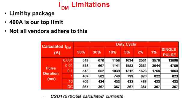
However, if we refer to the datasheet of a 30-volt CSD17570Q5B MOSFET, it provides us the current data ratings that we could reach at, if we tried to ignore the 400 amps cap. Which means that for example, the 1% duty cycle, 100-microsecond pulse period value shown in the datasheet would in fact correspond to a mammoth 3,500 amps, which looks unpracticable. Right?
And this is exactly why the pulse currents is limited to 400 amps. Furthermore, that's also the reason why the datasheet SOA will be usually be tied to the 400 amps limit. Not every suppliers might comply with this specifications. So, in case you happen to come across a supplier datasheet that provides an unbelievably high pulse current capacity, this could be based on just pure hypothetical calculation, rather than the package limitations on that value.
Original Source: ti.com-training
gilmoreyouresser1972.blogspot.com
Source: https://www.homemade-circuits.com/understanding-mosfet-current-rating-in-datasheets/
Postar um comentário for "What is Continuous Drain Current on a Mosfet"